
DNP Accelerates Development of Photomask Manufacturing Process for 2nm Generation EUV Lithography
Participate in NEDO R&D Project as Rapidus subcontractor
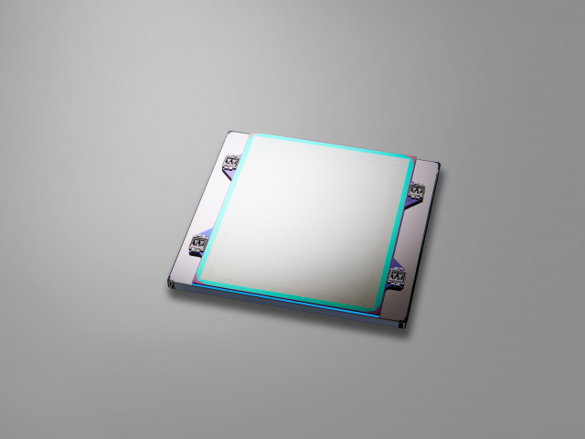
Image of EUV lithography with pellicle, a protective film for the photomask (Photo: Business Wire)
TOKYO--(뉴스와이어)--Dai Nippon Printing Co., Ltd. (DNP, TOKYO: 7912) has begun development of a photomask manufacturing for 2-nanometer (10-9 meter) generation logic semiconductors that support Extreme Ultra-Violet (EUV) lithography, the cutting-edge process for semiconductor manufacturing.
DNP will also act as a subcontractor and provide the newly developed technology to Tokyo-based Rapidus Corporation (Rapidus). Rapidus is participating in the Research and Development Project of the Enhanced Infrastructures for Post-5G Information and Communication Systems instigated by the New Energy and Industrial Technology Development Organization (NEDO).
[Background]
We have strengthened our ability to manufacture cutting-edge semiconductors with high productivity and quality. And in 2016, DNP was the world’s first merchant photomask manufacturer to introduce the multi-beam mask writing tool (MBMW).
In 2023, we completed the development of a photomask manufacturing process for 3-nm generation EUV lithography, and commenced development of 2-nm generation technology. In response to the need for further miniaturization, we will begin full-scale development of a photomask manufacturing process for 2-nm generation EUV lithography, including the operation of second and third multi-electron beam mask lithography systems in FY 2024.
DNP plans to bring online its second and third MBMW mask lithography systems in FY 2024, accelerating the development of photomasks for 2-nm generation EUV lithography.
DNP will act as a subcontractor on Development of Advanced Semiconductor Manufacturing Technology (Commissioned) by Rapidus as part of the NEDO’s previously mentioned R&D project.
[Going Forward]
By FY 2025, DNP will complete the development of a manufacturing process for photomasks for 2-nm generation logic semiconductors that support EUV lithography. From FY 2026 onwards, we will push ahead with the establishment of production technology with a view to commencing mass production in FY 2027.
We have also begun development with an eye toward the 2-nm generation and beyond, and have signed an agreement with imec, a cutting-edge international research organization headquartered in Leuven, Belgium, to jointly develop next-generation EUV photomasks. DNP will continue to contribute to the growth of Japan’s semiconductor industry by promoting development in collaboration with various partners within the framework of the international semiconductor industry.
About DNP
DNP was established in 1876, and has become a leading global company that leverages print-based solutions to engineer fresh business opportunities while protecting the environment and creating a more vibrant world for all. We capitalize on core competencies in microfabrication and precision coating technology to provide products for the display, electronic device, and optical film markets. We have also developed new products, such as vapor chamber and reflect array that offer next-generation communication solutions for more people-friendly information society.
View source version on businesswire.com: https://www.businesswire.com/news/home/20240319148117/en/